
How do solar panels work?
First let us Introduce the working principle of solar panels, with the global energy increasingly tense, solar energy as new energy has been vigorously developed, in which we use the most in life is solar cells. Solar cells are mainly made of semiconductor materials. Photoelectric conversion occurs when photoelectric materials absorb light energy to produce current.
What is the working principle of solar cells? Solar cells are devices that directly convert sunlight energy into electricity through photoelectric or photochemical effects. When sunlight shines on a semiconductor, some of it is reflected off the surface and the rest is absorbed or transmitted by the semiconductor. Some of the absorbed light, of course, becomes hot, while others collide with the valence electrons of the atoms that make up the semiconductor, producing electron-hole pairs. In this way, light energy is converted into electric energy by the form of electron-hole pairs.
1, The physical basis of solar cells
When the sun illuminates the p-n junction, the electrons in the semiconductor emit electrons because they have obtained the light energy, and the electron-hole pairs are produced accordingly. Under the action of the barrier electric field, the electrons are driven to the type region, and the holes are driven to the P type region, so that there are surplus electrons in the area, and there are surplus holes in the P region. Thus, the photoelectric field opposite to the potential electric field is formed near the p-n junction.
If a P-N junction exists in a semiconductor, a barrier electric field will be formed at both sides of the P-N junction, which can drive electrons to the N region and holes to the P region. As a result, there are surplus electrons in the N region and holes in the P region.
There are more than ten kinds of semiconductor materials that make solar cells, so there are many kinds of solar cells. At present, the most mature and commercially valuable solar cell is a silicon solar cells. Next, we take the silicon solar cell as an example to introduce in detail the working principle of solar cells.
1). Intrinsic semiconductor
The conductivity of matter depends on the atomic structure. Conductors are generally low-valent elements, and their outermost electrons easily break away from the nucleus and become free electrons. Under the action of an external electric field, they produce directional movement, forming an electric current. High-valent elements (such as inert gases) or polymers (such as rubber), their outermost electrons are strongly bound by the nucleus, it is difficult to become free electrons, so conductivity is very poor, become insulators. Silicon (Si) and germanium (Ge) are tetravalent elements, and their outermost electrons are neither as easily free from the bonds of nuclei as conductors, nor as tightly bound by nuclei as insulators, so their conductivity is between them.
A pure semiconductor is made into a single crystal through a certain process, namely an intrinsic semiconductor. Atoms in crystals form orderly arrays in space, and adjacent atoms form covalent bonds.
Covalent bonds in crystals have strong binding force, so at room temperature, only a few valence electrons get enough energy due to thermal motion (thermal excitation), thus breaking the bond into free electrons. At the same time, a hole is left in the covalent bond. The atom is positively charged by losing a valence electron, or the hole is positively charged. In intrinsic semiconductors, free electrons and holes appear in pairs, that is, the number of free electrons and holes is equal.
If free electrons meet holes in the process of motion, they will fill holes and disappear at the same time. This phenomenon is called recombination. At a certain temperature, the number of pairs of free electrons and holes produced by the intrinsic excitation is equal to the number of pairs of compound free electrons and holes, so the dynamic equilibrium is achieved.

Band theory:
a, When the electrons in a single atom move around the nucleus, the electrons in each orbit have their own specific energy.
b, The closer to the nuclear orbit, the lower the electron energy.
c, According to the principle of minimum energy, electrons always occupy the lowest level of energy.
d, The energy band occupied by valence electrons is called the valence band.
e, There is a forbidden band above the valence band. There is no energy level occupied by electrons in the forbidden band.
f, Above the forbidden band, is the conduction band. The energy level in the conduction band is the energy level that the valence electron can occupy when it breaks away from the covalent bond.
g, The forbidden bandwidth is expressed by Eg, and its value is related to the material and temperature of the semiconductor. T=300K, Eg=1.1eV of silicon, Eg=0.72eV of germanium.
2). Impurity semiconductor
Impurity Semiconductor: Impurity Semiconductor can be obtained by adding a small number of impurity elements into the intrinsic semiconductor through the diffusion process.
N-type and P-type semiconductors can be formed according to the impurity elements doped, and the conductivity of the impurity semiconductors can be controlled by controlling the concentration of the impurity elements doped.
N-type semiconductors: N-type semiconductors are formed by adding pentavalent elements (such as phosphorus) to pure silicon crystals to replace silicon atoms in the lattice.
Because the impurity atom has five valence electrons in its outermost layer, it has one more electron besides forming a covalent bond with the silicon atom around it. The electrons are free from covalent bonds and become free electrons. In N-type semiconductors, the concentration of free electrons is higher than that of holes, so the free electrons are called majority carriers and the holes are minority carriers. Because impurity atoms can provide electrons, they are called donor atoms.
P-type semiconductors: pure silicon crystals doped with trivalent elements (such as boron), so that it replaces the position of silicon atoms in the lattice, the formation of a P-type semiconductor.
Because the outermost layer of the impurity atom has three valence electrons when they form a covalent bond with the surrounding silicon atom, a “vacancy” is created, and when the outermost layer of the silicon atom fills the vacancy, a hole is created in the covalent bond. Therefore, in P semiconductor, holes are many and free electrons are few. Because the vacancies in impurity atoms absorb electrons, they are called acceptor atoms.

3). PN junction
PN junction: PN junction is formed at the interface of P-type semiconductor and N-type semiconductor fabricated on the same silicon wafer by different doping process.
Diffusion motion: A substance always moves from a place of high concentration to a place of low concentration. This motion due to the difference in concentration is called diffusion motion.
When a P-type semiconductor and an N-type semiconductor are fabricated together, the concentration of the two carriers varies greatly at their interfaces, so the hole in the P-region must diffuse to the N-region. Meanwhile, the free electrons in the N-region must diffuse to the P-region, as shown in the figure.
Because the free electrons diffuse into the P region recombine with the holes, and the holes diffused into the N region recombine with the free electrons, the concentration of many electrons decreases near the interface, the negative ion region appears in the P region, and the positive ion region appears in the N region. They can’t move, which is called the space charge region, thus forming the built-in electric field-epSILon;
As the diffusion proceeds, the space charge region widens and the built-in electric field strengthens. The direction of the built-in electric field points from the N region to the P region, which prevents the diffusion from proceeding.
Drift motion: under the action of electric field force, the motion of carriers is called drift motion.
When the space charge region is formed, the minority carrier drifts, the hole moves from the N region to the P region, and the free electron moves from the P region to the N region. In the absence of an external electric field and other excitations, the number of multiple particles participating in the diffusion motion is equal to the number of few particles participating in the drift motion, thus achieving a dynamic equilibrium and forming a PN junction, as shown in the figure. At this time, the space charge region has a certain width, the potential difference is =Uho, and the current is zero.
2, the principle of solar cells
1). Photovoltaic effect:
The photovoltaic energy conversion of solar cells is based on the photovoltaic effect of semiconductor PN junction. As mentioned earlier, photons with energy greater than the silicon forbidden band pass through the antireflective film into silicon when illuminated by a semiconductor photovoltaic device, and photogenerated electron-hole pairs are excited in N, depletion and P regions.
Depletion Zone: The photogenerated electron-hole pairs are separated by the built-in electric field immediately after they are generated in the depletion zone. The photogenerated electrons are fed into the N zone and the photogenerated holes are pushed into the P zone. According to the depletion approximation condition, the carrier concentration at the boundary of the depletion region is approximately 0, that is, p=n=0.
In the N region, the photogenerated holes diffuse to the P-N junction boundary after the photogenerated electron-hole pairs are formed. Once they reach the P-N junction boundary, they are immediately affected by the built-in electric field. They are pulled by the electric field force and drift across the depletion region into the P region. The photogenerated electrons (polyelectrons) are left in the N region.
In the P region, photogenerated electrons (minority electrons) enter the N region first because of diffusion and then because of drift, and photogenerated holes (polyelectrons) remain in the P region. The accumulation of positive and negative charges on both sides of the P-N junction results in the storage of excess electrons in the N region and the remaining holes in the P region. Thus forming a photoelectric field opposite to the built-in electric field.
a, In addition to partially counteracting the effect of the barrier electric field, the photovoltaic field also makes the P region positive and the N region negative, and the electromotive force is generated in the thin layer between the N region and the P region, which is called photovoltaic effect. When the battery is connected to a load, the photocurrent flows from the P region to the N region through the load, and the power output is obtained from the load.
b, If the ends of P-N junctions are opened, the electromotive force can be measured, which is called open-circuit voltage Uoc. For crystalline silicon batteries, the typical value of open-circuit voltage is 0.5 ~ 0.6V.
c, If the external circuit is short-circuited, there is a current in the external circuit which is proportional to the incident light energy. This current is called short-circuit current Inc.
Factors affecting photocurrent:
a, The more electron-hole pairs produced by light in the interface layer, the greater the current.
b, The more light energy the interfacial layer absorbs, the larger the area of the interfacial layer, i.e. the cell, and the larger the current formed in the solar cell.
c, Photoinduced carriers can be generated in the N region, depletion region and P region of solar cells.
d, The photogenerated carriers in each region must pass through the depletion region before recombination to contribute to the optical current. Therefore, the generation and recombination, diffusion and drift in each region must be taken into account in solving the actual photogenerated current.
Equivalent circuit, output power and fill factor of solar cells
A,Equivalent circuit
In order to describe the working state of the battery, the battery and load system are often simulated by an equivalent circuit.
a, Constant Current Source: Under constant illumination, a working solar cell, its photocurrent does not change with the working state, in the equivalent circuit can be regarded as a constant current source.
b, Dark current Ink: A part of the photocurrent flows through the load RL, and a terminal voltage U is established at both ends of the load. In turn, it is positively biased in the PN junction, causing a dark current Ibk opposite to the optical current.
c, In this way, the equivalent circuit of an ideal PN homogenous junction solar cell is plotted as shown in the figure.
d, Series resistance RS: Because of the front and back electrodes contact, and the material itself has a certain resistivity, base and top layer are inevitably introduced additional resistance. The current flowing through the load will inevitably cause loss when passing through them. In the equivalent circuit, the total effect can be represented by a series resistance RS.
e, Parallel resistance RSh: Because of the leakage of the battery edge and the metal bridge formed at the cracks and scratches when making the metalized electrode, the part of the current should be short-circuited through the load. This effect can be equivalent to a parallel resistance RSh.
When the current flowing into the load RL is I and the terminal voltage of the load RL is U, it can be obtained:
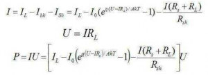
The P in the formula is the output power of the solar cell irradiated on the load RL.
B, Output power
When the current flowing into the load RL is I and the terminal voltage of the load RL is U, it can be obtained:
The P in the formula is the output power of the solar cell irradiated on the load RL.
When the load RL changes from 0 to infinity, the output voltage U changes from 0 to U0C and the output current changes from ISC to 0. Thus the load characteristic curve of solar cells can be drawn. Any point on the curve is called the working point. The connection between the working point and the origin is called the load line. The reciprocal of the slope of the load line is equal to RL. The horizontal and vertical coordinates corresponding to the working point are the working voltage and the working current.
When the load resistance RL is adjusted to a certain value Rm, a point M is obtained on the curve. The product of the corresponding working current IM and the working voltage Um is the largest, that is, Pm = ImUm.
Generally speaking, M point is the best working point (or maximum powerpoint), IM is the best working current, Um is the best working voltage, Rm is the best load resistance, and Pm is the maximum output power.
C,Fill factor
a, The ratio of maximum output power to (Uoc *Isc) is called fill factor (FF), which is one of the important indicators to measure the output characteristics of solar cells.
b, Filling factor characterizes the quality of solar cells. Under certain spectral irradiance, the larger the FF, the more square the curve, and the higher the output power.
D, solar cell efficiency, factors affecting the efficiency
(1). Solar cell efficiency:
When a solar cell is irradiated, the ratio of the output power to the incident light power is called the efficiency of the solar cell, also known as the photoelectric conversion efficiency. Generally refers to the maximum energy conversion efficiency when the external circuit is connected with the best load resistance RL.
In the above formula, if Ats are replaced by Aa (also called active area), that is, the area of grid lines is deducted from the total area, so the calculation efficiency is higher. This should be noted when reading the literature at home and abroad.
Prince of the United States first calculated the theoretical efficiency of silicon solar cells by 21.7%. In the 1970s, M. Wolf discussed it in detail. He also found that the theoretical efficiency of silicon solar cells was 20% ~ 22% under the AM0 spectral condition, and then modified it to 25% (AM1.0 spectral condition).
To estimate the theoretical efficiency of a solar cell, all possible losses from incident light to output power must be taken into account. Some of these losses are related to materials and processes, while others are determined by basic physical principles.
